(China (Mainland))

Product Summary
(1)The architecture of the XC161 combines advantages of RISC, CISC, and DSP;
(2)processors with an advanced peripheral subsystem in a very well-balanced way.
(3)addition, the on-chip memory blocks allow the design of compact systems-on-silicon with;
(4)maximum performance (computing, control, communication).
(5)The on-chip memory blocks (program code-memory and SRAM, dual-port RAM, data;
(6)SRAM) and the set of generic peripherals are connected to the CPU via separate buses.;
(7)Another bus, the LXBus, connects additional on-chip resoures as well as external;
(8)resources (see Figure 3).
(9)This bus structure enhances the overall system performance by enabling the concurrent;
(10)operation of several subsystems of the XC161.
(11)The following block diagram gives an overview of the different on-chip components and;
(12)of the advanced, high bandwidth internal bus structure of the XC161.
Parametrics
1.Maximum Rating Parameter:
Parameter Symbol Limit Values Unit Notes min. max.
Storage temperature TST-65 150C Junction temperature TJ-40 150C under bias Voltage on VDDI pins with
respect to ground (VSS)VDDI-0.5 3.25 V Voltage on VDDP pins with respect to ground (VSS)
VDDP -0.5 6.2 V Voltage on any pin with respect to ground (VSS)VIN -0.5 VDDP+ 0.5V
Input current on any pin during overload condition-10 10 mA Absolute sum of all input currents during overload
condition |100| m
2.Package Parameters (P-TQFP-144-19:
Parameter Symbol Limit Values Unit Notes min. max.Power dissipation PDISS 0.8 W ,Thermal Resistance RTHA 閳?32 K/W Chip-Ambien
3.Operating Condition Parameters
Parameter Symbol Limit Values Unit Notes min. max.Digital supply voltage for the core VDDI
2.35 2.7 V Active mode,fCPU = fCPUmax fCPUmax= 40 MHz for devices marked 0F, fCPUmax= 20 MHz for devices marked 0F.
Digital supply voltage for IO pads VDDP 4.4 5.5 V Active mode,External circuitry must guarantee low level at the RSTIN pin at least until both power supply voltages have
reached the operating range.
3)The specified voltage range is allowed for operation. The range limits may be reached under extreme operating
conditions. However, specified parameters, such as leakage currents, refer to the standard operating voltage
range of VDDP = 4.75 V to 5.25 V.Supply Voltage Difference VDD -0.5 V VDDP - VDDI
4)This limitation must be fulfilled under all operating conditions including power-ramp-up, power-ramp-down, and
power-save modes.Digital ground voltage VSS 0 V Reference voltage,Overload current IOV -5 5 mA Per IO pin
5)-2 5 mA Per analog input pin
6)Overload current coupling factor for analog inputs
7)KOVA 1.0 10-4 IOV > 0 1.5 10-3 IOV < 0 Overload current coupling factor for digital I/O pins
8)KOVD 5.0 10-3 IOV > 0 1.0 10-2 IOV < 0 Absolute sum of overload currents|IOV| 50 mA
9)External Load Capacitance CL 50 pF Pin drivers in default mode
10)Ambient temperature TA 0 70C SAB-XC161-40 85 C SAF-XC161-40 125 C SAK-XC161.
Features
(1) High Performance 16-bit CPU with 5-Stage Pipeline;
(2) 25 ns Instruction Cycle Time at 40 MHz CPU Clock (Single-Cycle Execution);
(3) 1-Cycle Multiplication (16 16 bit), Background Division (32) 16 bit) in 21 Cycles;
(4) 1-Cycle Multiply-and-Accumulate (MAC) Instructions;
(5) Enhanced Boolean Bit Manipulation Facilities;
(6) Zero-Cycle Jump Execution;
(7) Additional Instructions to Support HLL and Operating Systems;
(8) Register-Based Design with Multiple Variable Register Banks;
(9) Fast Context Switching Support with Two Additional Local Register Banks;
(10) 16 Mbytes Total Linear Address Space for Code and Data;
(11) 1024 Bytes On-Chip Special Function Register Area (C166 Family Compatible); (
(12) 16-Priority-Level Interrupt System with 74 Sources, Sample-Rate down to 50 ns;
(13) 8-Channel Interrupt-Driven Single-Cycle Data Transfer Facilities via;
(14) Peripheral Event Controller (PEC), 24-Bit Pointers Cover Total Address Space;
(15) Clock Generation via on-chip PLL (factors 1:0.15 1:10), or;
(16) via Prescaler (factors 1:1 60:1);
(17) On-Chip Memory Modules;
(18) 2 Kbytes On-Chip Dual-Port RAM (DPRAM);
(19) 4 Kbytes On-Chip Data SRAM (DSRAM);
(20) 2 Kbytes On-Chip Program/Data SRAM (PSRAM);
(21) 128 Kbytes On-Chip Program Memory (Flash Memory);
(22) On-Chip Peripheral Modules;
(23) 12-Channel A/D Converter with Programmable Resolution (10-bit or 8-bit) and;
(24) Conversion Time (down to 2.55 s or 2.15s);
(25) Two 16-Channel General Purpose Capture/Compare Units (32 Input/Output Pins);
(26) Multi-Functional General Purpose Timer Unit with 5 Timers;
(27) Two Synchronous/Asynchronous Serial Channels (USARTs); (28)Two High-Speed-Synchronous Serial Channels;
(29) On-Chip TwinCAN Interface (Rev. 2.0B active) with 32 Message Objects;
(30) (Full CAN/Basic CAN) on Two CAN Nodes, and Gateway Functionality;
(31) Serial Data Link Module (SDLM), compliant with J1850, supporting Class 2;
(32) IIC Bus Interface (10-bit addressing, 400 kbit/s) with 3 Channels (multiplexed);
(33) On-Chip Real Time Clock, Driven by Dedicated Oscillator;
(34) Idle, Sleep, and Power Down Modes with Flexible Power Management;
(35) Programmable Watchdog Timer and Oscillator Watchdo;
(36) Up to 12 Mbytes External Address Space for Code and Data;
(37) Programmable External Bus Characteristics for Different Address Ranges;
(38) Multiplexed or Demultiplexed External Address/Data Buses;
(39) Selectable Address Bus Width;
(40) 16-Bit or 8-Bit Data Bus Width;
(41) Five Programmable Chip-Select Signals;
(42) Hold- and Hold-Acknowledge Bus Arbitration Support;
(43) Up to 99 General Purpose I/O Lines,;
(44) partly with Selectable Input Thresholds and Hysteresis;
(45) On-Chip Bootstrap Loader;
(46) Supported by a Large Range of Development Tools like C-Compilers,;
(47) Macro-Assembler Packages, Emulators, Evaluation Boards, HLL-Debuggers,;
(48) Simulators, Logic Analyzer Disassemblers, Programming Boards;
(49) On-Chip Debug Support via JTAG Interface;
(50) 144-Pin TQFP Package, 0.5 mm (19.7 mil) pitc.
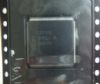
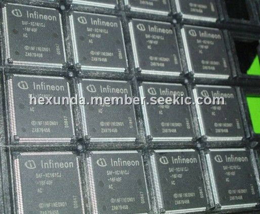
| Image | Part No | Mfg | Description |  |
Pricing (USD) |
Quantity | ||||||||
|---|---|---|---|---|---|---|---|---|---|---|---|---|---|---|
 |
 SAF-XC161CJ-16F40F BB |
Infineon Technologies |
16-bit Microcontrollers (MCU) 16 BIT SNGL CHIP 5V 40MHz Flash |
Data Sheet |
|
|
||||||||
|
SAF-XC161CJ-16F40FBB |
Infineon Technologies |
16-bit Microcontrollers (MCU) 128KB Flash 8 KB RAM 2xASC 2xSSC SDLM I2C |
Data Sheet |
Negotiable |
|
||||||||