(China (Mainland))

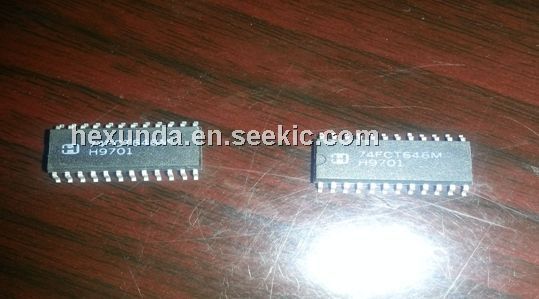
Product Summary
Description:The CD74FCT646 three-state octal bus transceiver/register uses a small geometry BiCMOS technology. The output
stage is a combination of bipolar and CMOS transistors that limits the output HIGH level to two diode drops below VCC.
This resultant lowering of output swing (0V to 3.7V) reduces power bus ringing (a source of EMI) and minimizes VCC bounce and ground bounce and their effects during
simultaneous output switching. The output configuration also enhances switching speed and is capable of sinking 64 milliamperes.
This device is a bus transceiver with D-Type flip-flops which act as internal storage registers on the LOW to HIGH transition of either CAB or CBA clock inputs. Output Enable (OE) and Direction (DIR) inputs control the transceiver functions.Data present at the high impedance output can be stored in either register or both but only one of the two buses can be
enabled as outputs at any one time. The Select controls (SAB and SBA) can multiplex stored and transparent (real time) data. The Direction control determines which data bus will receive data when the Output Enable (OE) is LOW. In the high impedance mode (Output Enable HIGH), A data can be
stored in one register and B data can be stored in the other register. The clocks are not gated with the Direction (DIR) and Output Enable (OE) terminals; data at the A or B terminals can be clocked into the storage flip-flops at any time
Parametrics
Absolute Maximum Ratings :
DC Supply Voltage (VCC) . . . . . . . . . . . . . . . . . . . . . . . . -0.5V to 6V
DC Diode Current, IIK (For VI< -0.5V) . . . . . . . . . . . . . . . . . . -20mA
DC Output Diode Current, IOK (for VO < -0.5V) . . . . . . . . . . . -50mA
DC Output Sink Current per Output Pin, IO . . . . . . . . . . . . . . .70mA
DC Output Source Current per Output Pin, IO . . . . . . . . . . . . -30mA
DC VCC Current (ICC) . . . . . . . . . . . . . . . . . . . . . . . . . . . . . .140mA
DC Ground Current (IGND). . . . . . . . . . . . . . . . . . . . . . . . . . .528mA
Features
Features
(1) Buffered Inputs;
(2) Typical Propagation Delay: 6.8ns at VCC = 5V,TA = 25℃, CL = 50pF;
(3) Noninverting;
(4) SCR Latchup Resistant BiCMOS Process and Circuit Design;
(5) Speed of Bipolar FAST?/AS/S;
(6) 64mA Output Sink Current;
(7) Output Voltage Swing Limited to 3.7V at VCC = 5V;
(8) Controlled Output Edge Rates;
(9) Input/Output Isolation to VCC;
(10) BiCMOS Technology with Low Quiescent Power
Diagrams