(China (Mainland))

Product Summary
The Virtex-4 Family is the newest generation FPGA from Xilinx. The innovative Advanced Silicon Modular Block or ASMBL column-based architecture is unique in the programmable logic industry. Virtex-4 FPGAs contain three families (platforms): LX, FX, and SX. Choice and feature combinations are offered for all complex applications. A wide array of hard-IP core blocks complete the system solution. These cores include the PowerPC processors (with a new APU interface), Tri-Mode Ethernet MACs, 622 Mb/s to 11.1 Gb/s serial transceivers, voltage/temperature system monitor blocks,dedicated DSP slices, high-speed clock management circuitry, and source-synchronous interface blocks. The basic Virtex-4 building blocks are an enhancement of those found in the popular Virtex-based product families: Virtex, Virtex-E, Virtex-II, Virtex-II Pro, and Virtex-II Pro X, allowing upward compatibility of existing designs. Virtex-4 devices are produced on a state-of-the-art 90-nm copper process, using 300 mm (12 inch) wafer technology. Combining a wide variety of flexible features, the Virtex-4 family enhances programmable logic design capabilities and is a powerful alternative to ASIC technology.
Features
1 Three families LX/SX/FX
- Virtex-4 LX: High-performance logic applications solution
- Virtex-4 FX: High-performance, full-featured solution for embedded platform applications
- Virtex-4 SX: High-performance solution for Digital Signal Processing (DSP) applications
2 Xesium? Clock Technology
- Digital Clock Manager (DCM) blocks
- Additional Phase-Matched Clock Dividers (PMCD)
- Differential Global Clocks
3 XtremeDSP? Slice
- 18x18, two complement, signed Multiplier
- Optional pipeline stages
- Built-In Accumulator (48-bits) & Adder/Subtracter
4 Smart RAM Memory Hierarchy
- Distributed RAM
- Dual-Port 18-Kbit RAM blocks Optional pipeline stages Optional programmable FIFO logic - Automatically remaps RAM signals as FIFO signals
- High-speed memory interface support: DDR and DDR-2 SDRAM, QDR-II, RLDRAM-II, and FCRAM-II
5 SelectIO Technology
- 1.5 to 3.3 V I/O Operation
- Built-In ChipSync? Source-Synchronous Technology
- Digitally-controlled impedance (DCI) active termination
- Fine grained I/O banking (Configuration in one bank)
6 Flexible Logic Resources
7 Built-in System Monitor (voltage/temp. measurement)
8 10-bit, 200kSPS A/D Converter (ADC)
9 Secure Chip AES Bitstream Encryption
10 90-nm copper CMOS process
11 1.2V core voltage
12 Flip-Chip Packaging
13 RocketIO 622 Mb/s to 11.1 Gb/s Multi-Gigabit Transceivers (MGT) (FX only)
14 IBM PowerPC RISC Processor Core (FX only)
- PowerPC 405 (PPC405) Core
- Auxiliary Processor Unit Interface (User Coprocessor)
15 Multiple Tri-Mode Ethernet MACs (FX only)
| Image | Part No | Mfg | Description |  |
Pricing (USD) |
Quantity | ||||||
|---|---|---|---|---|---|---|---|---|---|---|---|---|
 |
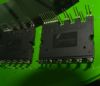
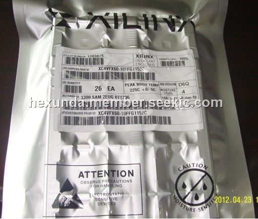
 XC4VFX60-10FFG1152C |
|
IC FPGA VIRTEX-4 FX 60K 1152FBGA |
Data Sheet |
|
|
||||||
| Image | Part No | Mfg | Description | |
Pricing (USD) |
Quantity | ||||||
|
XC4VFX100-10FF1152I |
|
IC FPGA VIRTEX-4FX 1152FFBGA |
Data Sheet |
|
|
||||||
|
XC4VFX100-10FF1517I |
|
IC FPGA VIRTEX-4FX 1517FFBGA |
Data Sheet |
|
|
||||||
|
XC4VFX100-10FFG1152C |
|
IC FPGA VIRTEX-4FX 100K 1152FBGA |
Data Sheet |
|
|
||||||
|
XC4VFX100-10FFG1152I |
|
IC FPGA VIRTEX-4FX 100K 1152FBGA |
Data Sheet |
|
|
||||||
|
XC4VFX100-10FFG1517C |
|
IC FPGA VIRTEX-4FX 100K 1517FBGA |
Data Sheet |
|
|
||||||
|
XC4VFX100-10FFG1517I |
|
IC FPGA VIRTEX-4FX 100K 1517FBGA |
Data Sheet |
|
|
||||||